Original Link: https://www.anandtech.com/show/15178/qualcomm-announces-snapdragon-865-and-765-5g-for-all-in-2020-all-the-details
Qualcomm Announces Snapdragon 865 and 765(G): 5G For All in 2020, All The Details
by Andrei Frumusanu on December 4, 2019 1:50 PM EST- Posted in
- Qualcomm
- Smartphones
- Mobile
- SoCs
- 7nm
- 5G
- Snapdragon 865
- Snapdragon 765
We’re here in Maui for the second day of Qualcomm’s fourth annual Snapdragon summit, for what is probably the most exciting part of the event, as we cover the disclosure of the intricate details of the brand new Snapdragon 865 and 765 SoCs that the company had briefly announced yesterday.
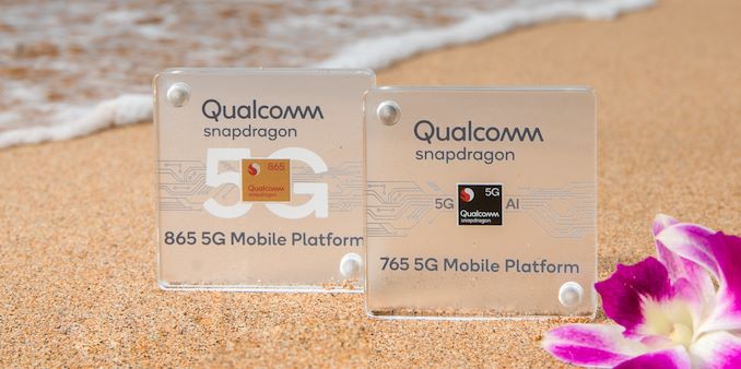
Indeed, this year, Qualcomm isn’t launching just one SoC, but rather two new platforms at the same time. The Snapdragon 865 is self-explanatory in its positioning; as a direct successor to the Snapdragon 855 we expect the new chip to represent the best Qualcomm is able to deliver, and be the silicon that powers most of 2020’s flagship devices. The new top-model this year is accompanied by the new Snapdragon 765 and 765G SoCs. As with other 7-series models since the launch of the new range, the new generation adds of the new features introduced with the new Snapdragon 865, at a lower performance level and a more affordable price for what is becoming an increasingly popular device category.
| Qualcomm Snapdragon Flagship SoCs 2019-2020 | |||
| SoC |
Snapdragon 865 |
Snapdragon 855 | |
| CPU | 1x Cortex A77 @ 2.84GHz 1x512KB pL2 3x Cortex A77 @ 2.42GHz 3x256KB pL2 4x Cortex A55 @ 1.80GHz 4x128KB pL2 4MB sL3 @ ?MHz |
1x Kryo 485 Gold (A76 derivative) @ 2.84GHz 1x512KB pL2 3x Kryo 485 Gold (A76 derivative) @ 2.42GHz 3x256KB pL2 4x Kryo 485 Silver (A55 derivative) @ 1.80GHz 4x128KB pL2 2MB sL3 @ 1612MHz |
|
| GPU | Adreno 650 @ ? MHz +25% perf +50% ALUs +50% pixel/clock +0% texels/clock |
Adreno 640 @ 585 MHz |
|
| DSP / NPU | Hexagon 698 15 TOPS AI (Total CPU+GPU+HVX+Tensor) |
Hexagon 690 7 TOPS AI (Total CPU+GPU+HVX+Tensor) |
|
| Memory Controller |
4x 16-bit CH @ 2133MHz LPDDR4X / 33.4GB/s or @ 2750MHz LPDDR5 / 44.0GB/s 3MB system level cache |
4x 16-bit CH @ 1866MHz LPDDR4X 29.9GB/s 3MB system level cache |
|
| ISP/Camera | Dual 14-bit Spectra 480 ISP 1x 200MP or 64MP with ZSL or 2x 25MP with ZSL 4K video & 64MP burst capture |
Dual 14-bit Spectra 380 ISP 1x 48MP or 2x 22MP |
|
| Encode/ Decode |
8K30 / 4K120 10-bit H.265 Dolby Vision, HDR10+, HDR10, HLG 720p960 infinite recording |
4K60 10-bit H.265 HDR10, HDR10+, HLG 720p480 |
|
| Integrated Modem | none (Paired with external X55 only) (LTE Category 24/22) DL = 2500 Mbps 7x20MHz CA, 1024-QAM UL = 316 Mbps 3x20MHz CA, 256-QAM (5G NR Sub-6 + mmWave) DL = 7000 Mbps UL = 3000 Mbps |
Snapdragon X24 LTE (Category 20) DL = 2000Mbps 7x20MHz CA, 256-QAM, 4x4 UL = 316Mbps 3x20MHz CA, 256-QAM |
|
| Mfc. Process | TSMC 7nm (N7P) |
TSMC 7nm (N7) |
|
We’ll start off with the whole story on the Snapdragon 865, and in particular one surprising aspect what we didn’t expect from the SoC this year; its lack of an integrated modem, and what the story behind the design choice.
No Modem Integration This Year?
The one aspect of the new Snapdragon 865 that overshadows all other new characteristics is the fact that Qualcomm designed it without an integrated modem. Qualcomm already announced this change yesterday during the day 1 of the event, without much context into the matter. It’s been fun seeing the reactions of various media and commenters theorising as to why this would be. It’s also one of the very first aspects that we wanted to have clarified by Qualcomm:
The choice to not integrate the modem this year was a highly practical one, stemming from the complexity of 5G and the platform. There are actually more nuances to this though, and one thing that Qualcomm wants to make clear, is that this isn’t just a matter of the company's technical ability to actually create a chip with an integrated 5G modem; it’s keen to point out the Snapdragon 765, also announced today, which does exactly this.
Instead, the technical difficulty of the 5G modem platform is actually on the platform and device side itself. As this will be the very first wide-range 5G implementation of a lot of OEM vendors who use Qualcomm’s chips, there will be a large number of designs who will be integrating 5G for the first time. The problem is that this requires a quite large development increase for the vendors creating the devices: they need to make sure their RF systems, antenna designs, as well as certifications of the systems are in full order. The nature of the 5G design complexity means that this process in a device’s development cycle this time around is actually quite a lot more complicated and more time-consuming than what we’ve seen from past 4G phones.
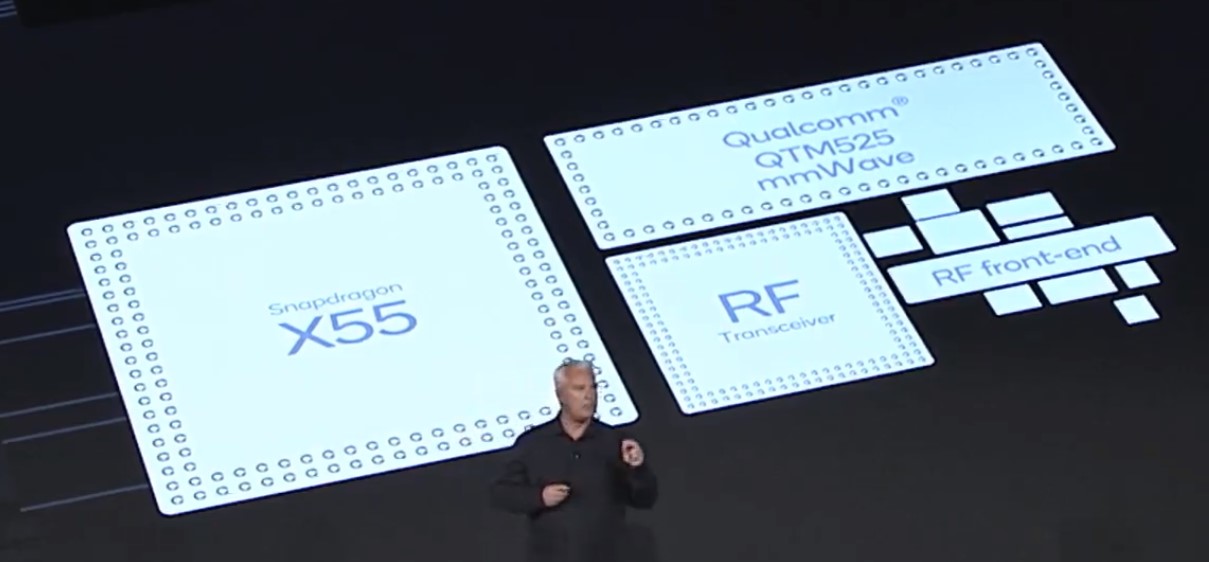
Qualcomm’s solution to the problem, in order to facilitate the vendor’s device development cycle, is to separate the modem from the rest of the application processor, at least for this generation. The X55 modem has had a lead time to market, being available earlier than the Snapdragon 865 SoC by several months. OEM vendors thus would have been able to already start developing their 2020 handset designs on the X55+S855 platform, focusing on getting the RF subsystems right, and then once the S865 becomes available, it would be a rather simple integration of the new AP without having to do much changes to the connectivity components of the new device design.
Qualcomm’s explanation makes a lot of sense in practical terms, and would bring time-to-market advantages. The company explains that in the future, it would re-integrate the modem back into the SoC, and this generation’s choices just made more sense for today’s situation in the market. Qualcomm isn’t the only one to have made such a choice, Samsung’s Exynos 990 SoC makes the same exact design decisions, shipping the main SoC as a simple application processor without any modem, although we don’t have any official backstory on their rationale for the design choice.
The decision of shipping AP+discrete modem does have some disadvantages though. Motherboard PCB complexity does go up this generation, more so than competitors solutions which are able to integrate 5G modems (Such as the HiSilicon Kirin 990 5G, or the MediaTek Dimensity 1000). We also expect some compromises in terms of battery efficiency due to the silicon overhead, however as a counter-argument, Apple’s iPhones always have had separate AP+modem solutions, and the latest generation this year had amongst the strongest battery life performance of any device out there, even with a competing Intel modem.
As for the X55 modem itself: It’s the same piece that Qualcomm announced earlier this year, and this time around promises full global 5G connectivity ability (the X50’s support was more limited). The modem chip is manufactured on the TSMC’s 7nm process node, and the most important fact about the new combination is that the Snapdragon 865 SoC is exclusively tied to the X55 modem. This means that Qualcomm is selling the 865 SoC only as a pair with the X55 modem, and they do not offer support with any past 4G modem. In theory vendors could use another modem, but since they only sell the new platform as a pair anyway, it would make very little sense for anybody to do this.
One question that also came up is on whether vendors, for whatever reason, would still be able to develop 4G phones with the Snapdragon 865+X55 platform. Qualcomm says this would be possible if you essentially just ignore the X55’s 5G capabilities, but they don’t see any reason for any vendor to actually do this. In essence, bar any abnormal decision from some vendors, all Snapdragon 865 devices in 2020 will be full 5G devices.
The Snapdragon 865 Application Processor: TSMC 7nm N7P
With the elephant in the room of the modem configuration being out of the way, we come to the actual Snapdragon 865 application processor.
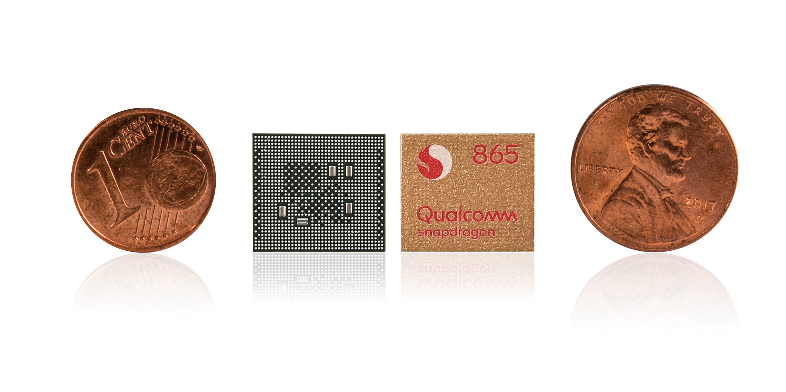
For me, the biggest surprise of the new chipset was Qualcomm’s revelation that the chip is the fact that it’s manufactured by TSMC on the improved 7nm “N7P” node – this is the same manufacturing process as used by Apple’s A13 chipset. For the longest time were expecting this generation to be manufactured on Samsung’s 7nm EUV process (7LPP), given as the two companies had announcement nearly 2 years ago. It seems that the announcement was actually about the new Snapdragon 765, which does come on the 7LPP process node, and which we'll be covering in more detail later on in the article.
Qualcomm only's comment is that their process node choices were based on various considerations, including volume. Reading between the lines, it’s possible that Qualcomm wasn’t as confident in Samsung’s ability to manufacture the large quantities needed for the new chip. I’ve also heard murmurs from other sources that Samsung’s process simply doesn’t have as good performance and leakage characteristics as TSMC, and in flagship parts, those aspects have to be taken higher consideration than in say a premium- or mid-range SoC. In any case, it’s a big blow to Samsung’s foundry business as having the design win this year was quite critical, as I do not expect them to win the 2021 flagship contract due to TSMC’s 5nm leadership.
As for the choice between TSMC’s N7P and N7+ (+ is the EUV node), it seems HiSilicon is currently the only client for the node for the time being, with the Kirin 990 5G being the only chipset manufactured on the node until later in 2020. It’s most likely that TSMC here simply doesn’t yet have the EUV volume capacity and yields to fulfil Qualcomm’s demand at this point in time, essentially being in a similar situation as Samsung, with the only difference being that TSMC has a viable high-volume DUV-based process ready as an alternative.
Cortex-A77 Cores, LPDDR5, Adreno 650 GPU
No More CPU Customisations For Now: Cortex-A77 Used
On the CPU side, the Snapdragon 865’s improvements over the Snapdragon 855 are very straightforward in terms of specifications:
| SoC |
Snapdragon 865 |
Snapdragon 855 |
| CPU | 1x Cortex A77 @ 2.84GHz 1x512KB pL2 3x Cortex A77 @ 2.42GHz 3x256KB pL2 4x Cortex A55 @ 1.80GHz 4x128KB pL2 4MB sL3 @ ?MHz |
1x Kryo 485 Gold (A76 derivative) @ 2.84GHz 1x512KB pL2 3x Kryo 485 Gold (A76 derivative) @ 2.42GHz 3x256KB pL2 4x Kryo 485 Silver (A55 derivative) @ 1.80GHz 4x128KB pL2 2MB sL3 @ 1612MHz |
We find the same 1+3+4 CPU configuration as found on the Snapdragon 855, using the same 2.84GHz, 2.4GHz and 1.8GHz clock frequencies, and the same 512KB, 256KB and 128KB L2 cache configurations.
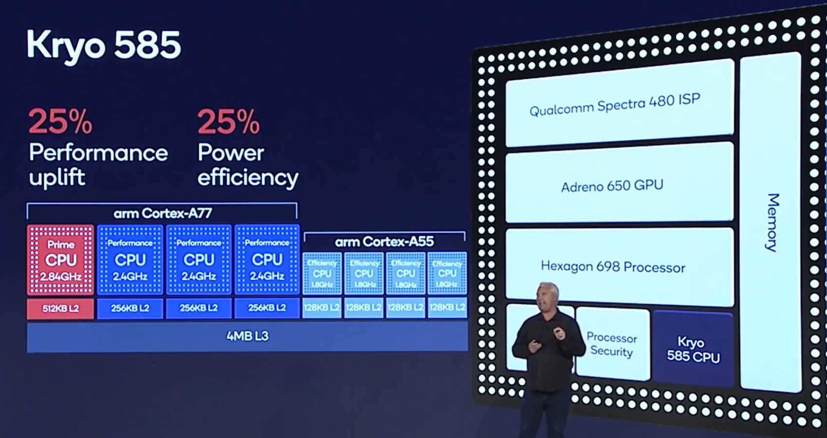
The big difference of course, that instead of using Cortex-A76 based cores in the S855, the new chipset is using Arm’s newest Cortex-A77 cores. A larger change in strategy this year is that while Qualcomm still uses the “Built-on-Cortex-technology” license to be able to customize some parts of the interface IP of the CPUs (And be able to brand it as the Kryo 585 parts), they’ve abandoned customisations on the CPU core itself. Qualcomm saw that the return on time investment with Arm to customise previous generations didn't result in as high returns as they would have hoped, and for the Snapdragon 865 they simply opted to use the default configuration Cortex-A77 as offered by Arm.
Still, the new CPU microarchitecture is said to be able to offer a 25% performance uplift this year, all of it which is essentially due to IPC improvements of the new design. As we had expected, we’re not seeing any clock improvements this year, and the CPU frequencies remain flat, reaching an identical 2.84GHz for the “Prime” core and 2.4GHz for the “Gold” cores.
Qualcomm claims a 25% power efficiency gain for the new SoCs, but this is an ISO-performance comparison against the previous generation (At equal performance to the S855, the S865 uses 25% less energy/power). In absolute terms at maximum performance, the new Snapdragon 865 big CPUs use more power to achieve their higher performance, meaning efficiency at peak perf is flat.
The Cortex-A55 cores remain practically the same, which to be honest are getting a bit long in the tooth as they’ve essentially not changed in 3 generations now. We’re very much overdue a large microarchitectural update from Arm as the yearly small efficiency core updates from Apple now put the Android SoCs to shame in regards to performance and efficiency.
One aspect that Qualcomm did finally improve on is the L3 cache of the CPU cluster, which has now been increased from 2MB to 4MB. While the performance benefits here are welcome, Qualcomm explains that the main reason for the change was increased power efficiency, reducing more expensive DRAM memory accesses in light workloads, which makes a lot of sense.
The Adreno 650 GPU: Similar Architecture, Wider Microarchticture
On the GPU side of things, we’re seeing Qualcomm make evolutionary changes to the new IP block. It’s actually a bit unusual for Qualcomm to remain in the 600-series this year and the company had never before stretched out an architecture over three generations like this.
| SoC |
Snapdragon 865 |
Snapdragon 855 |
| GPU | Adreno 650 @ ? MHz +25% perf +50% ALUs +50% pixel/clock +0% texels/clock |
Adreno 640 @ 585 MHz |
Qualcomm’s improvement claims for this generation come down to an aggregate of 25% over a variety of industry benchmarks and real workloads. It’s to be noted that the company did say we’ll be see higher improvements in some workloads, for example higher complexity tests such as Aztec might see a higher percentage.
Qualcomm's "Mobile GPU approaches to power efficiency"
@ High-Performance Graphics 2019
Earlier last summer Qualcomm did detail some titbits of its architecture, describing the ALUs execution units as being separate MUL+ADD units per lane, and also showcased some first-party performance metrics of the Adreno 640 GPU. The Adreno 630 and 640 were both 2-core GPUs with each respectively 256 and 384 ALUs per core based on the measured throughput. The Adreno 650 increasing this by 50% could either mean we’re seeing three 256-ALU cores, or that there’s now two 512-ALU cores. The resulting computational power at a hypothetical 600MHz clock rate would be ~1.2TFLOPs. We’ll have to wait and see where the frequency ends up at, Qualcomm didn't want to disclose it.
The Adreno 640 had made a huge jump in texture fillrate as it doubled up from the TMUs from 12 per core to 24 per core, for a total of 48. This resulted in quite the unusual 3:1 texel:pixel ratio in terms of fillrate capability. The Adreno 650 now increasing the ROPs by 50% means well see an increase from 8 per core (16 total) to 12 per core (24 total), bringing it back to a 2:1 balance, with the pixel fillrate capabilities now catching up to the Mali GPU counterparts.
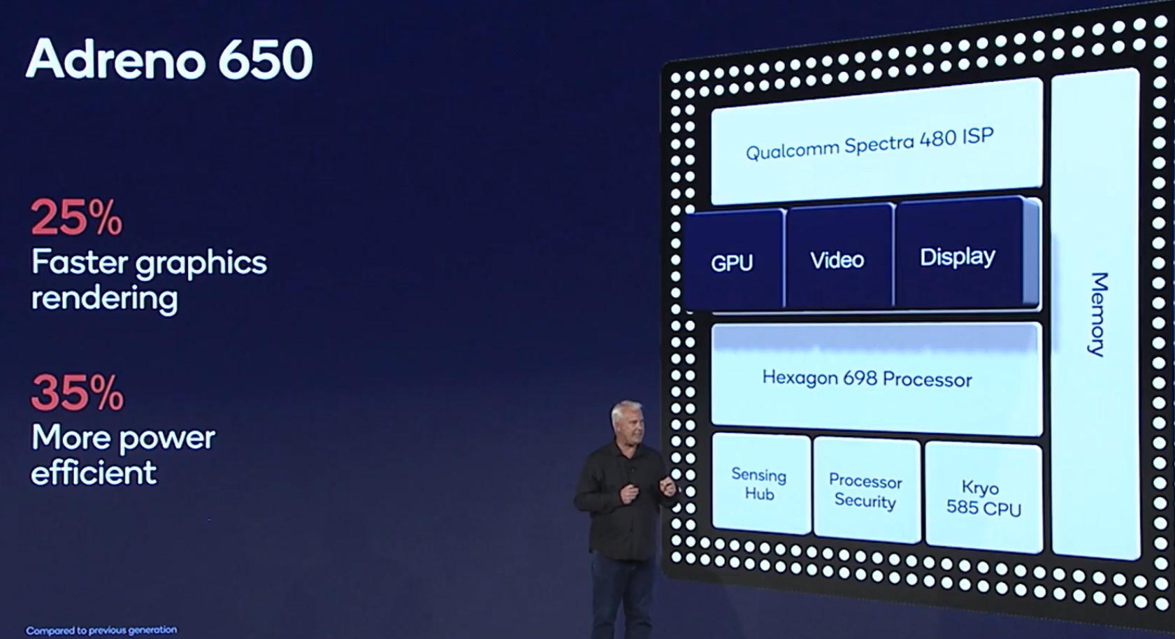
I asked about absolute power consumption, and the company discloses that it’ll be similar to the Snapdragon 855 in terms of peak power. There’s a slight contradiction here as the company also mentions that sustained performance is going to be a lot better than on the S855. It’s possible that we would be seeing larger performance improvements at lower than peak frequencies, and the company does say that at equal performance levels, the Adreno 650 is now 35% more efficient than its predecessor.
It was also a good opportunity to talk about the increasing peak power consumption over the last few generations. Back during the Snapdragon 835 days and earlier, Qualcomm’s SoCs were praised and took pride in being able to remain quite cool, with peak device active load power only being 3.5-4W. In more recent generations this has steadily increased, with the Snapdragon 855 now falling in at around 5W. Qualcomm explains that this was actually a change requested by OEMs who had improved the thermal dissipation capabilities of their device designs – telling the company that they are now able to handle higher power levels, and for Qualcomm to use that to increase performance.
I’m not too sure how to feel about this as it’s pretty much a double-edged sword and puts the responsibility of actually achieving the peak performance of the SoC solely in the hands of the device vendor, and them being able to properly design a good thermal solution. As we’ve already seen this year, some vendors are doing well in this regard, while others prioritise temperature over retaining higher performance levels. In any case, our unique testing methodology makes sure we’re exposing such differences in detail.
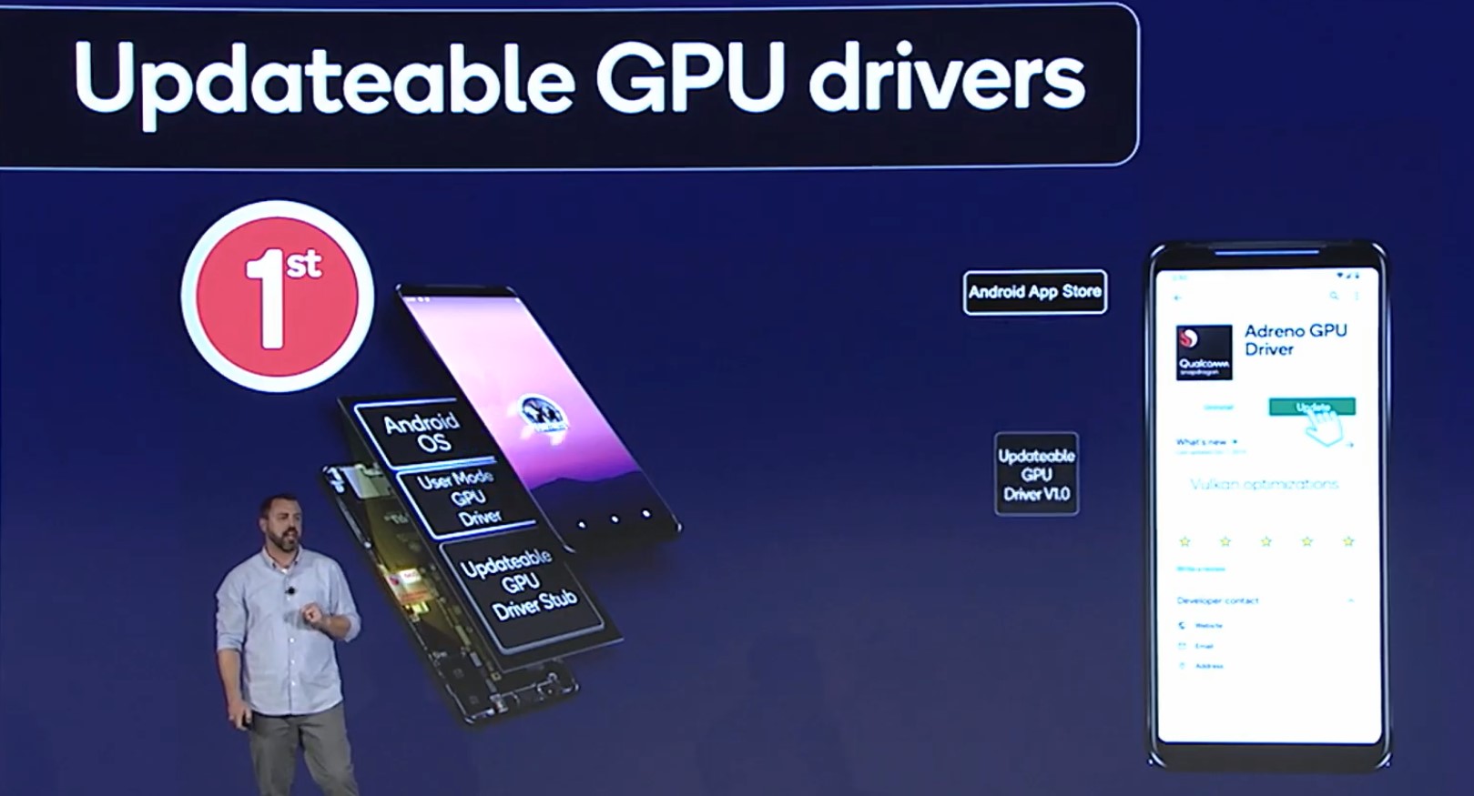
Unrelated to the hardware of the GPU, a big new improvement for the Adreno 650 and Snapdragon SoCs going forward is the fact that Qualcomm is now planning to distribute and update the graphics drivers over the Play Store. This feature was actually introduced to Android back in 2017 with Android 8/Oreo, but up until now no vendors actually ever took advantage of it, as it looks like it took time for vendors to make this feature operable with their BSPs. Qualcomm is now the first to achieve this, and the company is planning on quarterly GPU driver updates for new SoC generations going forward.
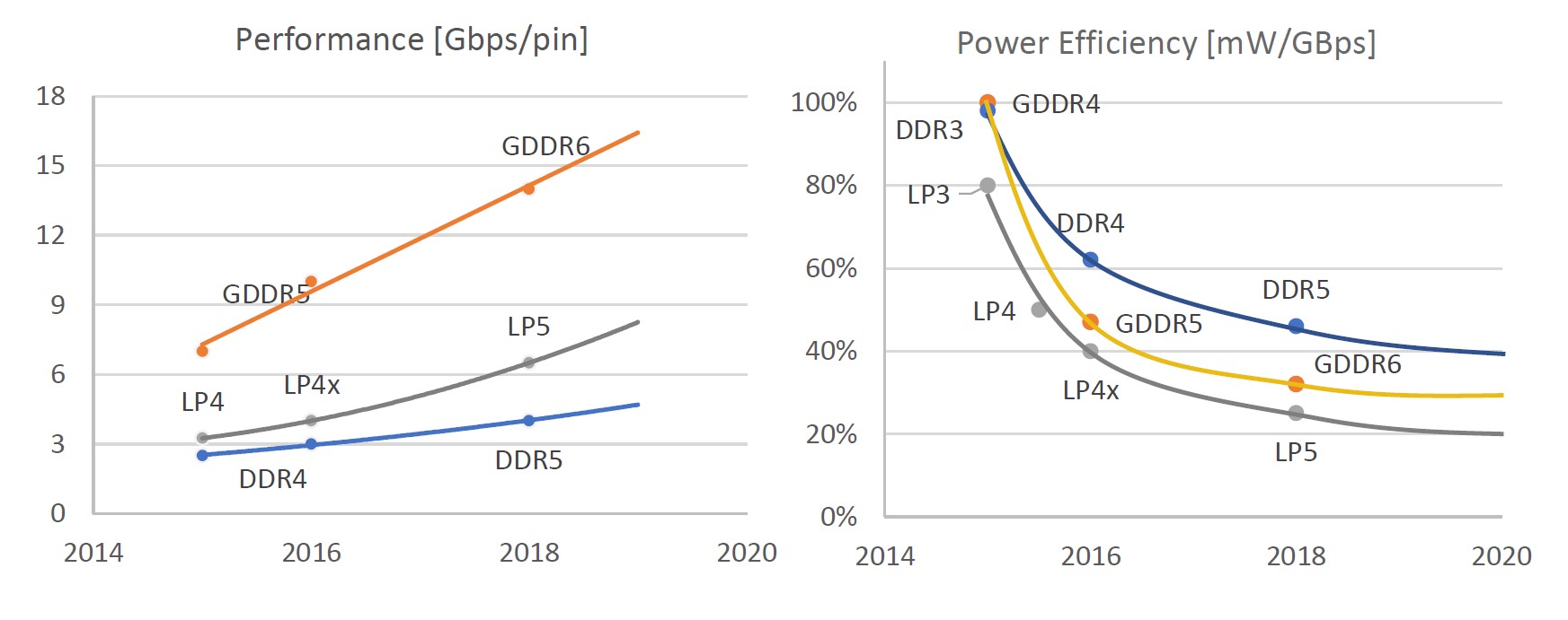
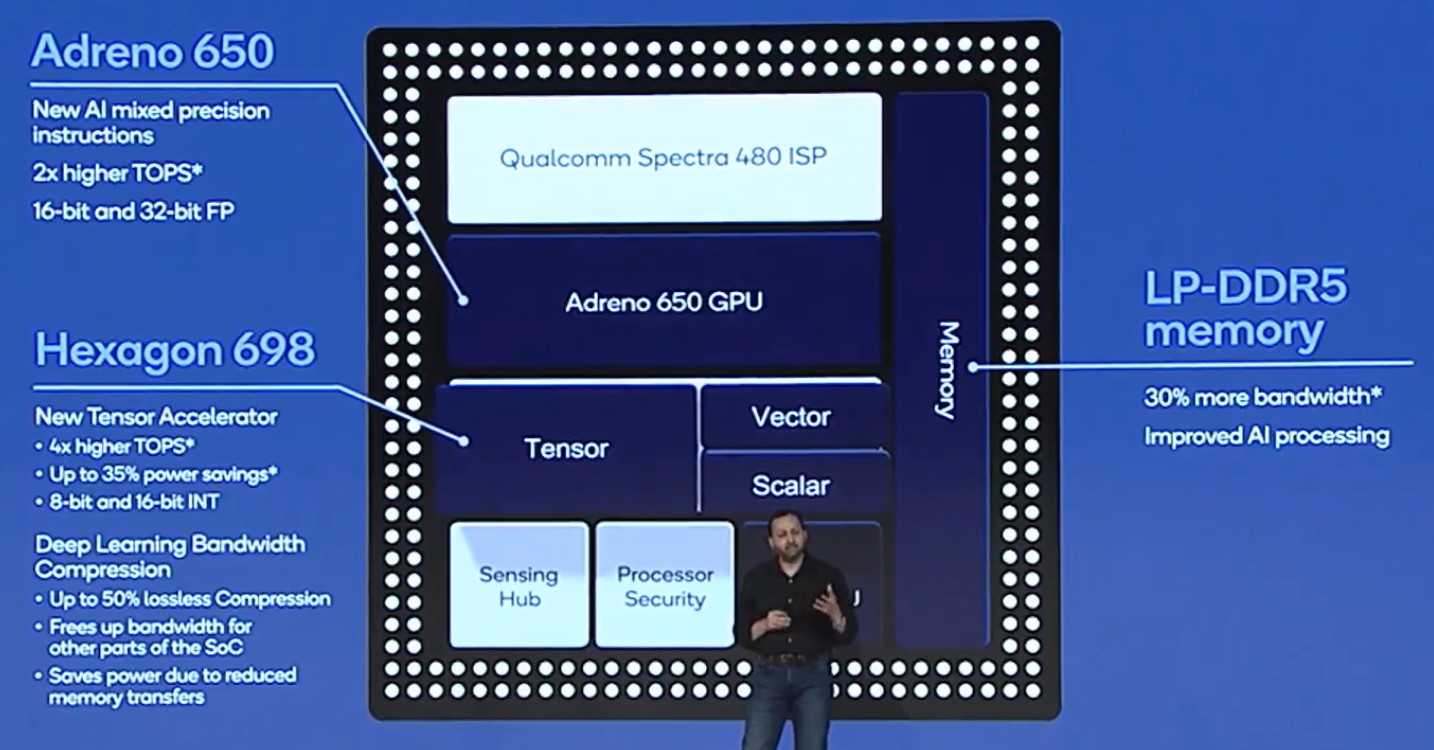
2020 Sees The Commercialisation of LPDDR5
2020 is the year where we’ll be seeing LPDDR5 being introduced to mobile. The new memory standard promises to improve the power efficiency per bit transferred by roughly 20%, and the Snapdragon 865 now comes with support for the new technology.
| SoC |
Snapdragon 865 |
Snapdragon 855 |
| Memory Controller |
4x 16-bit CH @ 2133MHz LPDDR4X / 33.4GB/s or @ 2750MHz LPDDR5 / 44.0GB/s 3MB system level cache |
4x 16-bit CH @ 2133MHz LPDDR4X 33.4GB/s 3MB system level cache |
What’s interesting here is that Qualcomm is using a hybrid memory controller, supporting both LP4X and LP5 memory standards. LPDDR4X is supported to up to 2133MHz, while LPDDR5 memory is supported 2750MHz (5500MHz effective considering DDR). The bandwidth improvement here is 31%, and Qualcomm notes that the two technologies will roughly offer the same memory latency, meaning no improvement nor degradation.
Surprisingly, Qualcomm sounded rather conservative in regards to the actual performance impact of the new technology. They do say that it will bring advantages in bandwidth starved situations, but the company’s representatives underplayed the impact that it will have. Qualcomm allows vendors to choose between LP4X and LP5 in their device implementations, and says the performance differences between the two would a few percentage points. The new memory technology is rather a matter of future-proofing the SoC as well as being able to support the memory as DRAM-manufacturers shift their production lines.
The company also said that they’ve improved the memory subsystem of the SoC and were able to lower latency to around “130ns”, although it’s not exactly clear what the context and percentage improvement here is – if it’s most likely a full random access test, in which case in comparison the S855 landed in at 150-170ns depending on memory depth, then that’s actually a quite notable and respectable improvement.
The system level cache of the SoC still falls in at 3MB this generation, the same as the previous generation. I questioned if it made sense to still maintain this at this size, especially in the face of now almost every vendor having a similar capability, and especially in the face of Apple’s humongous 16MB implementation in the A13. The company said that for their architecture and workloads that they’re seeing, they opted to retain the size, but are looking into the future to possibly increase it (Die area is probably a large consideration here, maybe expect an increase in the next process node?).
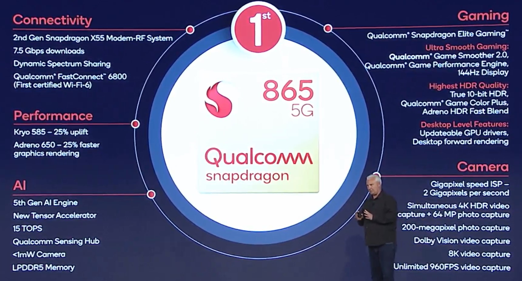
Immense AI, Camera and ISP Upgrades
New Hexagon 695 DSP: 4x Performance On New Tensor Cores - 15 TOPs Total on SoC
The Snapdragon 865 now ships with the new Hexagon 695 DSP block. The single biggest improvement of the new design is a massive quadrupling of the processing power of the dedicated tensor cores. This jump alone is able to double the SoC’s aggregate AI processing ability up from 7 TOPs to 15 TOPs.
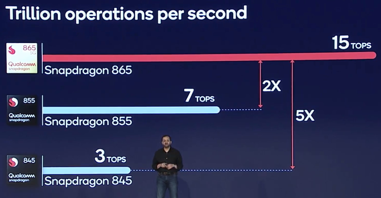
Qualcomm here still doesn’t properly do a breakdown between the IP blocks which contribute to this number, but given that the GPU only saw a ~20% increase, and that the Hexagon’s scalar and vector execution units this year have remained the same in terms of performance, we estimate that the tensor units now roughly come in at around 10TOPs by themselves.
Qualcomm has also now included lossless weight and activation compression for the Tensor cores, being able to reduce bandwidth consumption up to 50%. This is a similar feature we've seen advertised by third-party NPU IP offerings, only that Qualcomm is going to be shipping this now in a product in just a few months.
Power efficiency of the block is also have said to have improved by 35%, making computations less costly in terms of battery life.
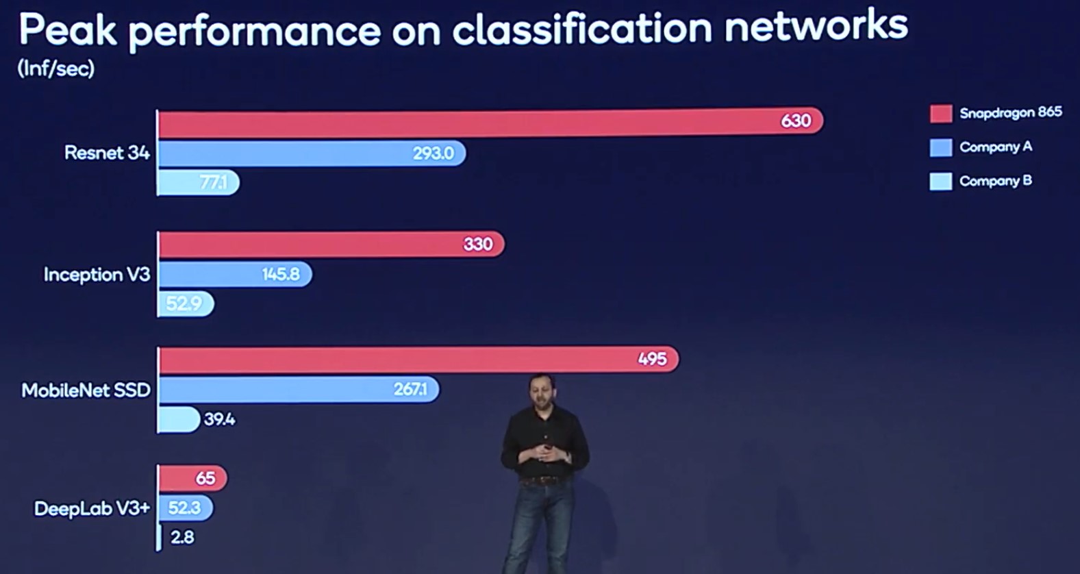
Qualcomm talks how about its inference performance and inference power efficiency is significantly higher than competing solutions. We don't know the comparison SoCs being showcased here, but a likely candidates here are the Apple A13 and the Kirin 990? It could also be an Exynos or other SoC.
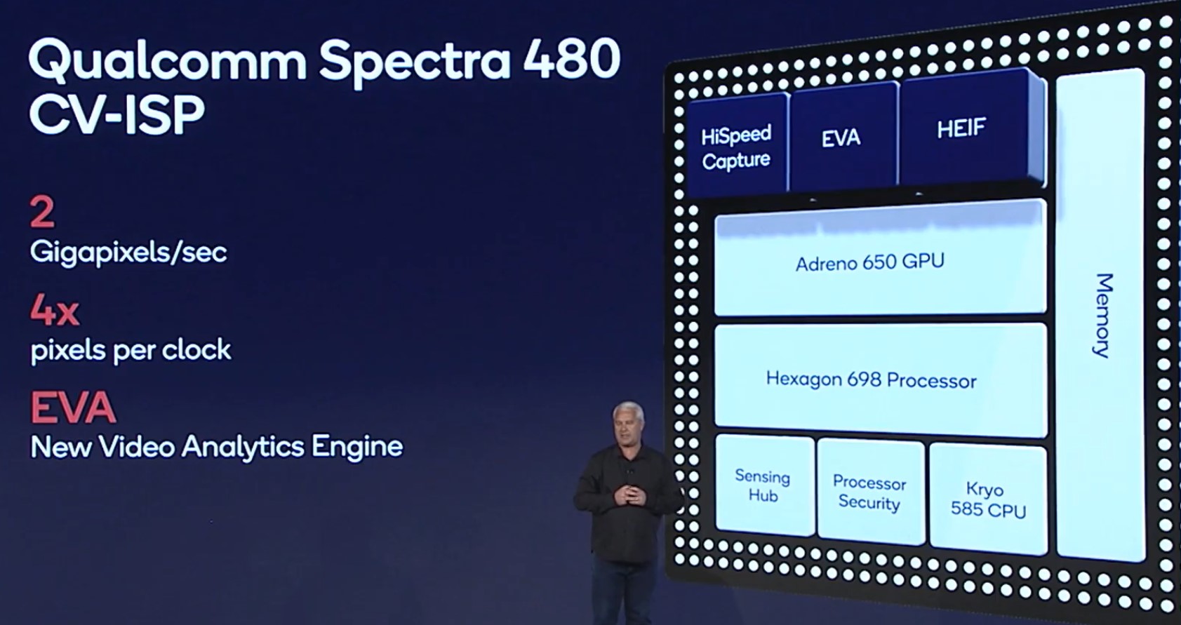
New Spectra CV-480 ISP: 2 Gigapixels/s Enabling Massive Sensors
Aside from its 5G abilities, it’s very much evident that camera is very much at the very centre of the Snapdragon 865’s new features. The whole camera subsystem has seen some massive upgrades in the IP, and amongst the biggest improvements in capability lies in the new Spectra 480 computer-vision ISP.
The new IP has seen a major architectural change in that it’s now able to process 4 pixels per clock instead of just only 1 PPC as in the previous generation. This has now massively upgraded the pixel processing throughput to 2 Gigapixels/second, allowing the SoC a wide variety of use-cases that in the past simply weren’t possible due to lack of raw power.
Starting off with video capture, the new SoC is able to now record in 4K HDR while simultaneously capturing up to 64MP still shots at the same time. But 4K video isn’t the limit anymore – and you even can say that in terms of framerate as now 4K120 recording is supported, but the Snapdragon 865 now supports 8K30 video recording.
Video recording quality continues to support all the features we’ve seen in the previous generation, meaning 10-bit and various HDR standards such as HLG, HDR10, HDR10+, but now the new SoC expands this even further with the introduction of the ability to do live recording in the Dolby Vision HDR standard. Qualcomm explains that the Snapdragon 865 not only is the first smartphone SoC to be able to do this, but it’s the first camera platform of any kind in the world, as usual Dolby Vision content right now is enabled post-capture in the editing room, rather being something that’s being natively recorded by a camera.
The new improved capabilities of the ISP and video encoder also erase some current recording limitations, for example, slow-motion video recording at 960fps is sustained indefinitely instead of being limited to a couple of seconds of real-time footage.
Although normally I wouldn’t have brought this up, MediaTek’s recent release of the Dimensity 1000 did recently popularise the discussion topic: No, the Snapdragon 865 doesn’t support the AV1 codec for video decoding. It looks like we’ll have to wait for the next generation for that.
In terms of still capture photography, the new ISP performance will now allow for support for sensors of up to 200MP, which actually don’t yet exist as Samsung’s recent 108MP behemoth is currently the largest of its class right now.
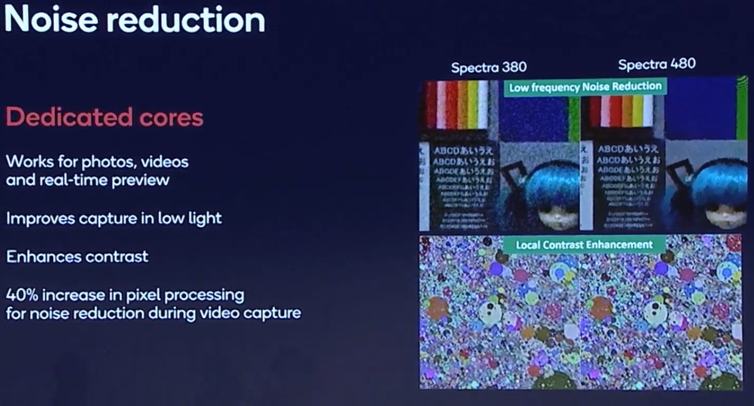
The new ISP now has various new functionalities in order to improve noise reduction and contrast enhancements. Particularly the new noise reduction features is said to be quite difficult to achieve.
Although Qualcomm advertises the 200MP figure predominantly, it’s to be noted that actual capture with zero shutter lag (ZSL) is limited to 64MP – so there is a rather larger compromise in capturing at resolutions beyond 64MP.
High Refresh Rate Displays Normalised: Support For 144Hz
Already some vendors are leading the pack in 2019, but we’re expecting 2020 to see wide-range adoption of high refresh-rate displays. Even more importantly, we’ll be seeing implementations at high resolutions higher than 90 and 120Hz, supporting up to 144Hz displays. Qualcomm explains that the barrier that’s been lifted here is the SoC’s Display Processing Unit (DPU) that has had its throughput significantly increased.
I asked the company about the impact on battery life and which component of a phone accounts for the highest power increases. Surprisingly, it’s not any one component, with most of them seeing pretty much just an evenly distributed linear increase in power requirements, with the actual display panel itself (excluding the DDIC), seeing actually the least increases in power draw.
The Snapdragon 765 SoC: Improved Premium With 5G
Alongside the main Snapdragon 865 star-SoC today, Qualcomm is also announcing a new addition to the 700-series line-up. To be exact, we’re seeing two new additions, the Snapdragon 765 and Snapdragon 765G. The two chips are of the same silicon, with a slight difference in performance binning, and are both successors to the Snapdragon 730.
| Qualcomm Snapdragon Premium SoCs 2019-2020 | |||
| SoC |
Snapdragon 765
|
Snapdragon 730 | |
| CPU | 1x Kryo 475 Prime (CA76) @ 2.3GHz (non-G) @ 2.4GHz (765G) 1x Kryo 475 Gold (CA76) @ 2.2GHz 6x Kryo 475 Silver (CA55) @ 1.8GHz |
2x Kryo 470 Gold (CA76) @ 2.2GHz 6x Kryo 470 Silver (CA55) @ 1.8GHz |
|
| GPU | Adreno 620 +20% perf (non-G) +38% perf (765G) |
Adreno 618 | |
| DSP / NPU | Hexagon 696 HVX + Tensor 5.4TOPS AI (Total CPU+GPU+HVX+Tensor) |
Hexagon 688 HVX + Tensor |
|
| Memory Controller |
2x 16-bit CH @ 2133MHz LPDDR4X / 17.0GB/s |
2x 16-bit CH @ 1866MHz LPDDR4X 14.9GB/s |
|
| ISP/Camera | Dual 14-bit Spectra 355 ISP 1x 192MP or 36MP with ZSL or 2x 22MP with ZSL |
Dual Spectra 350 ISP 1x 36MP with ZSL or 2x 22MP with ZSL |
|
| Encode/ Decode |
2160p30, 1080p120 H.264 & H.265 10-bit HDR pipelines |
||
| Integrated Modem | Snapdragon X52 Integrated (LTE Category 24/22) DL = 1200 Mbps 4x20MHz CA, 256-QAM UL = 210 Mbps 2x20MHz CA, 256-QAM (5G NR Sub-6 4x4 100MHz + mmWave 2x2 400MHz) DL = 3700 Mbps UL = 1600 Mbps |
Snapdragon X15 LTE (Category 15/13) DL = 800Mbps 3x20MHz CA, 256-QAM UL = 150Mbps 2x20MHz CA, 64-QAM |
|
| Mfc. Process | Samsung 7nm EUV (7LPP) |
Samsung 8nm (8LPP) |
|
In terms of architecture, the new chips don’t differ as drastically to its predecessors as the flagship S865. On the CPU side, we’ve seen a slight change in the CPU layout, with the big cores now coming in a 1+1 Prime and Gold configuration, rather than an equal pairing as with the Snapdragon 730. We didn’t get more detailed info on the setup, but it’s likely that the new Prime core has larger L2 caches than the secondary big cores, if Qualcomm’s implementation here is similar to the larger flagship siblings. Clock frequencies on the Prime core have increased to 2.3GHz for the regular Snapdragon 765, whilst it goes up to 2.4GHz on the S765G. The secondary big core remains at 2.2GHz.
The big disappointment here is that these are still Cortex-A76 based CPU cores, so Qualcomm hasn’t actually updated the microarchitecture designs of the CPUs. In this regard, the new chip actually seems slightly inferior to the Exynos 980 with A77 cores, which targets the same device segment.
We continue to see 6x Cortex A55 cores at 1.8GHz alongside the big cores.
Qualcomm’s First Integrated 5G Modem
The biggest change in the SoC is the fact that this is Qualcomm’s first chipset to integrate a 5G modem. In terms of modem architecture, it’s said that the block is identical in functionality to the X55 external modem, just that it supports lesser bandwidth. 4G LTE speeds reach up to 1200Mbps download and 210Mbps upload, and 5G speeds aggregate over sub-6 as well as mmWave peak at 3700Mbps down and 1600Mbps up.
Qualcomm was keen to point out that unlike other vendors, they’re not skimping on mmWave connectivity at this category, although I do wonder if vendors will actually integrate mmWave modules on the devices with the SoC as it’s essentially a high-end feature on a more price-sensitive platform.
Also very interesting is the new SoC’s manufacturing process – it’s made by Samsung on their new 7nm EUV 7LPP node, meaning the premium SoC technically has a more advanced process technology than the flagship Snapdragon 865, although in practice this doesn’t necessarily mean it’s actually better in terms of characteristics.
The first Snapdragon 765(G) devices are expected to be released in the first quarter of 2020.
The Snapdragon 865 & 765: First Impressions
Overall, today’s launch was very exciting and hopefully we’ve been able to present to you with some exclusive clarifications on the new SoC platforms.
Qualcomm’s execution in recent years have been pretty much excellent, and flagship devices powered by Snapdragon SoCs have been always extremely well-rounded. Naturally we do wish the Android SoC vendors would put the pedal to the metal in terms of raw performance and efficiency and catch up with Apple’s designs, but when it comes to all other aspects of SoC design Qualcomm is in pretty much in a leadership role. That’s not to say the performance improvements of the new generation is disappointing, I’m expecting the new CPU cores to shine and Qualcomm has promises very healthy improvements in a generation where there have only been minor process node improvements.
Two big takeaways from today’s launch were camera and 5G. The camera capabilities of the Snapdragon 865 means that next year we’ll see some exciting new designs and a leap forward in camera capture experiences.
The Snapdragon 865 and 765 both supporting 5G to the fullest extend also means that the SoCs represent the foundation for 5G devices in 2020, and we expect vendors to 5G in their full line-up, with maybe only a few exceptions at the low and mid-low-range. I was quite doubtful about the value in buying X50 based 5G devices this year as they did have some crucial feature compromises, I don’t have the same qualms about the new X55 and X52 based platforms next year, and it’s likely the generation to get on board for 5G.
I’m excited to get my hands on the first Snapdragon 865 devices early next year, and hopefully we’ll be able to get more details on the platform in the next weeks and months to come.


